Boundary conditions and carriers
Two settings in the Simulation parameters panel decide how much of the doping you typed is actually electrically active — and, when you want to, let you set the carrier density directly instead.
01Temperature
Temperature is in kelvin and defaults to 300. It feeds everything that depends on thermal energy: the carrier distributions, the intrinsic concentration, and — unless you override it with the next setting — the fraction of your dopants that are ionised.
Set it deliberately rather than leaving it at room temperature out of habit. A structure that behaves one way at 300 K can behave quite differently at 77 K, and the difference is rarely subtle.
02FullyIonised
This checkbox is off by default, so EpiSolve uses partial ionisation unless you tell it otherwise.
- Unticked — each donor or acceptor is occupied according to Fermi–Dirac statistics and its binding energy from the nearest band edge. A fraction of your dopants stay neutral and contribute no charge.
- Ticked — every dopant is assumed ionised. The doping you typed is the charge you get.
03How much difference it makes
Freeze-out shows up in two parameters: temperature and doping. To illustrate the effect of temperature consider acceptors in GaAs, at a moderate 1017 cm−3:
300 K    89 % ionised
150 K    58 %
 77 K    17 %
 50 K     5 %
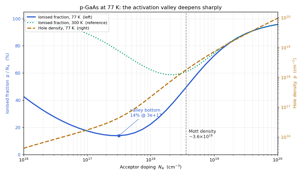
Doping is the other parameter, and the behaviour is not a simple relationship. Following GaAs acceptors on an ascending scale at 77 K:
10¹⁶     43 % ionised
10¹⁷     17 %   ← deepest freeze-out
10¹⁸     22 %
10¹⁹     73 %
10²⁰     96 %   ← effectively metallic
Freeze-out deepens with doping, bottoms out, and then reverses. The turning point is the Mott density — a few × 1018 cm−3 for acceptors in GaAs. Below this each dopant sits on its own isolated level and freezes out when cold; above it the dopant wavefunctions overlap into a band that merges with the valence band, so they stay ionised down to any temperature, exactly as a real degenerate contact does. EpiSolve models that crossover, so partial ionisation returns to full ionisation above the Mott density.
How deep the dopant sits decides where the crossover falls: a deeper level has a smaller orbit and so a higher Mott density, and freezes out to higher doping. Magnesium in GaN (0.23 eV) is the extreme case — its Mott density is so high that it stays largely un-ionised even at 1019 cm−3, which is much of why p-type GaN is hard to make.
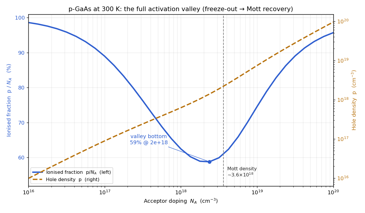
The activation valley — and why it is not a bug. The same dip and recovery happen at room temperature, only much shallower. Follow GaAs acceptors up the doping scale at 300 K and the active fraction falls before it climbs back:
5×10¹⁷     70 % active
2×10¹⁸     59 %   ← valley bottom (near the Mott density)
5×10¹⁸     64 %
1×10¹⁹     75 %
1×10²⁰     96 %   ← recovered, effectively metallic
The dip is a real effect, not a solver artefact. As dopant concentration rises toward the Mott transition, neighboring dopants’ overlapping wavefunctions and random potentials distort the band edge into a disordered tail of states. These sit close in energy to the conduction or valence band but remain spatially localised, so carriers reaching them stay effectively trapped rather than conducting, until the dopant concentration crosses the Mott density and the states delocalise into a true metallic band. Below that threshold, the fraction of “missing” carriers grows as the transition is approached, and is worst at low temperature, where there isn’t enough thermal energy to lift carriers into the mobile states. The effect is generally stronger for acceptors than donors.
Two things to bear in mind. It is a dip in the percentage, never in the carriers: the hole density rises monotonically with doping the whole way (5×10¹⁷ to 5×10¹⁸ is roughly nine times more holes, even as the percentage falls). And the valley bottom sits close to the Mott density — a few × 1018 cm−3 for GaAs acceptors — which is where the activation figure is most provisional and should be considered indicative rather than exact.
So at room temperature, away from the heaviest doping, the two settings agree closely and the default rarely causes trouble. Partial ionisation earns its keep when you go cold, at light-to-moderate doping, near the Mott density, or with a deep dopant.
04The doping column as a carrier concentration
Ticking the box has a second use that has nothing to do with accuracy. It makes the doping column a direct control on the free-carrier density: what you type is what the solver gets, net of any other factors. The column stops describing a dopant population and starts describing the carriers themselves.
That is what you want when you are working backwards from a measurement rather than forwards from a growth recipe. To extract a carrier concentration from a Hall measurement: put the measured mobility in the layer’s Mobility column, tick FullyIonised, and adjust the doping figure until the calculated sheet resistance matches the measured sheet resistivity. Because the solution accounts for the depleted regions at the surface and the interfaces, the figure you land on is the concentration in the part of the layer that is actually conducting — which is what a Hall measurement alone cannot separate from the thickness it is conducting through.
05Dopant depth
The layer table’s Dopant depth (eV) column overrides the material’s own binding energy for that layer. Leave it blank and the database value is used.
Two things to know about it. The value you enter is applied to the donor or the acceptor, dependent on which dopant column you have used for that layer. And it is ignored entirely when FullyIonised is ticked, since nothing then depends on where the level sits.
06Example structures to try
Everything on this page is easier to appreciate once you have seen these effects. A small set of ready-to-run structures ships with EpiSolve under File → Open Example → Semiconductor devices → Ionisation examples. Each is a single uniform layer with FullyIonised left off, so the point is the flat bulk deep in the layer: read the majority-carrier density there off the plot and divide by the doping to get the ionised fraction.
GaAs Acceptor 1e17 300K Active         89 %   shallow acceptor, warm — baseline
GaAs Acceptor 1e17 77K Frozen          17 %   the same layer, cooled
GaAs Acceptor 1e18 77K Mott Valley     22 %   in the freeze-out valley, below the Mott density
GaAs Acceptor 2e19 77K Mott Recovered  84 %   more doping, same 77 K — recovered
GaN Mg 2e20 300K Deep Frozen            1 %   deep acceptor, stays frozen
AlGaAs Si DX 1e18 300K Frozen          20 %   DX donor, resistive n-AlGaAs
They are arranged to walk through the page in order. The first two are the same p-GaAs layer at 300 K and 77 K — the cooling axis of section 03, 89 % down to 17 %. The three 77 K structures then climb the doping scale across the Mott density: 1018 sits in the valley (22 %), while 2×10¹⁹ has recovered (84 %) — the reversal that section 03 describes, in two structures you can open side by side. The last two are the cases that stay frozen: magnesium in GaN is a deep acceptor and holds at ~1 % even at 2×10²⁰, and the silicon donor in Al0.3GaAs is a DX centre, so n-AlGaAs comes out resistive where plain n-GaAs would be fully active — both illustrations of how far the dopant depth of section 05 reaches. Tick FullyIonised on any of them and it returns to ~100 %.
The setting applies to the whole structure, not to one layer. Partial ionisation follows the local doping: a heavily doped cap, above its Mott density, comes out fully ionised, while a lightly doped active region on the same structure still freezes out as it should.
That makes partial ionisation — the default — the safe general choice. Tick FullyIonised when you want the doping column to read as a carrier density directly (section 04), or to match another tool that assumes it — not because partial ionisation mishandles a degenerate contact.

